Kaynes Semicon supports multiple semiconductor packaging platforms designed for power, industrial, and emerging semiconductor applications.
EXCEL LEADFRAME
ELEVATE SUBSTRATE
EXPLORE ADVANCED
Packaging Platforms
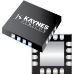
QFN – Quad Flat No-leads Packages
Leadless packages offering compactness, thermal efficiency, and versatility for a wide range of applications, with cost-effective manufacturing benefits.
SOT – Small Outline Transistor packages
Compact, surface-mount semiconductor solutions, ideal for space-constrained applications and automated assembly processes.
TO – Transistor Outline Packages
Robust through-hole packages for power semiconductors, featuring high power handling and effective thermal dissipation.
Applications include

Industrial control systems

Automation platforms

Embedded electronics
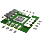
Semiconductor Modules
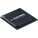
Flip Chip BGA
High-density integration with solder ball grid, ideal for microprocessors and memory devices.
FCBGA
Enhanced electrical performance and compact size with flip chip technology, suitable for graphics processors and data centers.
FCCSP
Compact chip scale package with flip chip technology, ideal for miniaturized electronics and mobile devices.
Applications include

AI compute systems

Edge processors

Communication platforms
Test and Validation
MCM – Multi-chip module Package
Compact multi-chip module for high-performance computing and telecommunications.
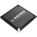
SIP – System in Package Solutions
Integration of multiple components for simplified system integration, perfect for IoT devices and wireless communication systems.
Co-Packages Optics
Optical components integrated within a single package, ideal for high-speed data transmission and telecommunications applications.
Applications include

EV powertrains

Industrial motor drives

Renewable energy systems
Discover the Kaynes Semicon Advantages for IC Packaging
Innovation Leaders
We are at the forefront of packaging innovation, constantly pushing boundaries to bring you the quality product and most advanced solutions.
Quality Assurance
Our rigorous testing processes and commitment to quality assurance ensure that your semiconductor devices meet the highest industry standards.
Global Reach, Local Commitment
With a global footprint, we seamlessly integrate into the semiconductor supply chain, providing efficient logistics and a reliable production network with a local commitment to your success.
Collaborative Partnership
Your success is our success. We believe in collaborative partnerships, working closely with you to achieve shared goals and milestones.